The semiconductor industry is rapidly approaching the need to fabricate sub-100 nano meter structures to continue performance increases in integrated circuits. Photolithography remains the enabling technology for the fabrication of integrated circuit patterns. Although industry is able to commercially produce 130 nano meter features, lithographic materials and processes are not fully available for the production of sub-100 nano meter structures. New materials must be able to produce structures with dimensional tolerances of 2 nano meters to 5 nano meters, dimensions near the size of the polymer chain molecules in the imaging layer.
Current imaging layers, chemically amplified photoresists, are multi-component materials consisting of a polymer resin initially insoluble in an aqueous base developer solution, a photoacid generator (P A G), and other additives. A schematic diagram of the fabrication process and an example structure are shown in Figures 1 and 2. The patterns are generated in the resist by exposure to U V radiation through a mask. In the exposed areas, the P A G decomposes, forming an acid species. Upon baking, the acid diffuses and catalyzes a deprotection reaction rendering the insoluble resist soluble in a developer. The soluble regions are then removed with the aqueous base developer. Control over this process is dominated by the events in the transitional region between exposed and unexposed areas of the photoresist.
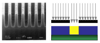
| Figure 1. At left, S E M image of a lithographically fabricated structure with a nominal critical dimension of 150 nano meter and 300 nano meter pitch. At right, schematic illustration of patterning through a mask to create the structure. |
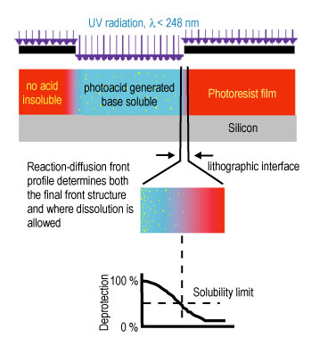
| Figure 2. Schematic diagram of the reaction-diffusion process in chemically amplified photoresists. The transitional region between exposed and unexposed regions is particularly important for critical dimension and roughness control. |
The initial development of chemically amplified photoresists was a key technological breakthrough furthering the continued use of optical photolithography for the fabrication of sub micro meter features. The importance of chemically amplified photoresist concepts is illustrated by the industry-wide use of these materials in the fabrication of state-of-the-art devices today and into the foreseeable future. With the imminent need for sub-100 nano meter feature sizes, nanometer level control over the spatial evolution of the deprotection reaction front and the subsequent development steps is needed. The current level of understanding of the acid-catalyzed reaction-diffusion process is not sufficiently detailed to achieve this goal.
To meet the need for spatially detailed data, we have developed, in collaboration with the IBM T. J. Watson Research Center and the University of Texas at Austin, an experimental methodology to directly measure the spatial evolution of the deprotection reaction front through each processing step. By using model photoresist polymers with a deuterated protection group, neutron and x-ray reflectivity (N R, X R) measurements are able to follow the compositional and density profiles of the reaction-diffusion process in an idealized transitional region in a bilayer film stack. Neutron contrast with the reaction is possible because the reaction products involving the deuterated protection group are volatile, as illustrated in Figure 3.
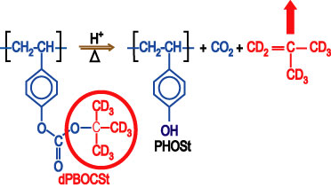
| Figure 3. General deprotection reaction in a chemically amplified photoresist. Deuterated molecular parts with strong contrast to neutrons are shown in red. |
The N R and X R results from a series of bilayer samples are shown in Figure 4. N R and X R measurements were taken after each processing step from the spin-coating of each film layer through exposure and bake to the dissolution of the upper layer and any deprotected polymer. The data show that the deprotection reaction front broadens with time within the photoresist. The initial interfacial width was approximately 4 nano meters wide whereas the reaction front was nearly 20 nano meters wide. Upon development, the data show that the developed film remained sharply defined with a surface roughness of approximately 4 nano meter as well. Although the reaction front was much wider than the final interfacial width, the selectivity of the dissolution process allows for the fabrication of well-defined nanostructures with diffusive transport mechanisms.
The spatial detail afforded by the developed methodology can play an important role in not only the qualitative description of the reaction-diffusion process, but also with the quantitative determination of physical parameters and changes in any physical or chemical properties over the nanometer length scales required for control over the fabrication of sub-100 nano meter structures. In addition, the strategy developed here is general and can be adapted for the study of candidate photoresist materials being developed for future applications. “[This work (Refer to reference 1)] opens a window of opportunity to construct structure-property relationships between chemical transport mechanisms and ultimate resist resolution. It may also lead to insights into the ultimate, intrinsic resolution limits and critical dimension control of polymer-based imaging materials.” (Refer to reference 2)
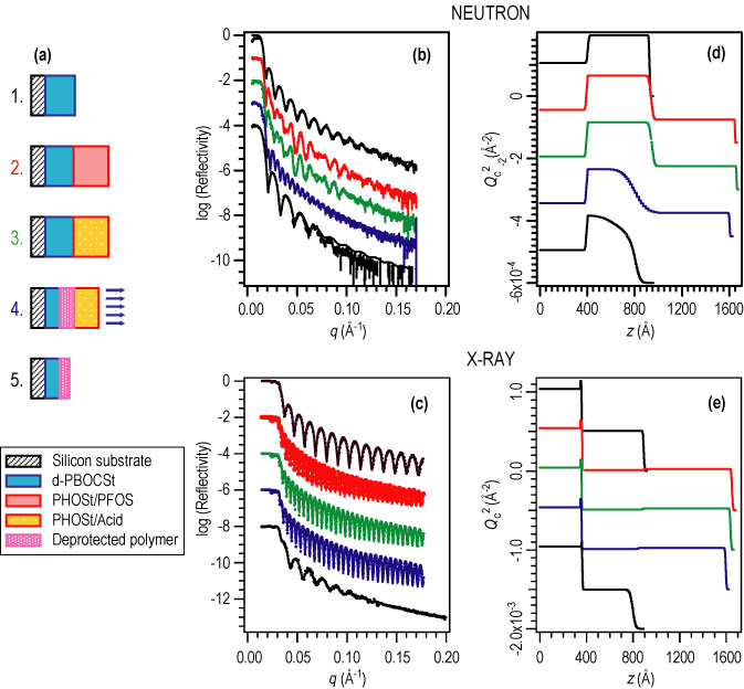
| Figure 4. (A) schematic diagram of the processing steps including the application of each film layer, exposure to U V radiation, a post-exposure bake (P E B) and development. (B) and (D) show the N R data and compositional depth profile and (C) and (E) show the X R data and density depth profiles from each step. |
References
[1] E. K. Lin, C. L. Soles, D. L. Goldfarb, B. C. Trinque, S. D. Burns, R. L. Jones, J. L. Lenhart, M. Angelopoulos, C. G. Willson, S. K. Satija, and W. L. Wu, Science, 297, 372 (2002).
[2] E. Reichmanis and O. Nalamasu, Science, 297, 349 (2002).
Authors
E. K. Lin, C. L. Soles, R. L. Jones, J. L. Lenhart, and Wen-li Wu
Polymers Division
National Institute of Standards and Technology
Gaithersburg, MD 20899-8541
S. K. Satija
NIST Center for Neutron Research
National Institute of Standards and Technology
Gaithersburg, MD 20899-8562
D. L. Goldfarb and M. Angelopoulos
IBM
T.J. Watson Research Center
Yorktown Heights, NY 10598
B. C. Trinque, S. D. Burns, and C. Grant Willson
University of Texas at Austin
Austin, TX 78712
Back to FY2002 HTML main page
Go to next article
To view all symbols correctly, please download Internet Explorer 6 or Netscape 7.1